Transistor-Transistor Logic (TTL)
Introduction to Logic Families:
Logic Gates like NAND, NOR are used in daily applications for performing logic operations. The Gates are manufactured using semiconductor devices like BJT, Diodes, or FETs. Different Gate’s are constructed using Integrated circuits. Digital logic circuits are manufactured depending on the specific circuit technology or logic families.
The different logic families are:
- RTL(Resistor Transistor Logic)
- DTL(Diode Transistor Logic)
- TTL(Transistor-Transistor Logic)
- ECL(Emitter Coupled Logic)
- CMOS(Complementary Metal Oxide Semiconductor Logic)
Out of these RTL and DTL are rarely used.
Features of Logic Families:
- Fan Out: Number of loads the output of a GATE can drive without effecting its usual performance. By load we mean the amount of current required by the input of another Gate connected to the output of the given gate.
- Power Dissipation: It represents the amount of power needed by the device. It is measured in mW. It is usually the product of supply voltage and the amount of average current drawn when the output is high or low.
- Propagation Delay: It represents the transition time which elapses when the input level changes. The delay which occurs for the output to make its transition is the propagation delay.
- Noise Margin: It represents the amount of noise voltage allowed at the
input, which doesn’t affect the standard output.
Introduction to TTLs:
It is a logical family consisting completely of transistors. It employs a transistor with multiple emitters. Commercially it starts with the 74 series like the 7404, 74S86, etc. It was built in 1961 by James L Bui and commercially used in logic design in 1963
Classification of TTL:
TTLs are classified based on the output.
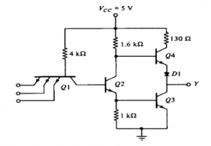
1. Open Collector Output: The main feature is that its output is 0 when low and floating when high. Usually, an external Vcc may be applied.
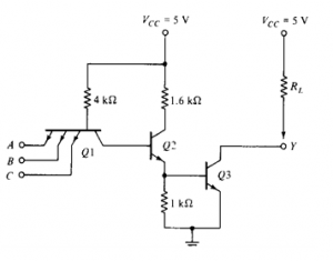
Transistor Q1 behaves as a cluster of diodes placed back to back. With any of the input at logic low, the corresponding emitter-base junction is forward biased and the voltage drop across the base of Q1 is around 0.9V, not enough for the transistors Q2 and Q3 to conduct. Thus the output is either floating or Vcc, i.e. High level.
Similarly, when all inputs are high, all base-emitter junctions of Q1 are reverse biased and transistor Q2 and Q3 get enough base current and are in saturation mode. The output is at logic low. (For a transistor to go to saturation, collector current should be greater than β times the base current).
Applications of open-collector output:
It is used in 3 major applications:
- In driving lamps or relays
- In performing wired logic
- In the construction of a common bus system
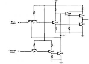
2. Totem Pole Output:
Totem Pole means the addition of an active pull up the circuit in the output of the Gate which results in a reduction of propagation delay.
Logic operation is the same as the open collector output. The use of transistors Q4 and diode is to provide quick charging and discharging of parasitic capacitance across Q3. The resistor is used to keep the output current to a safe value.
3. Three state Gate:
It provides 3 state output.
- Low-level state when a lower transistor is ON and an upper transistor is OFF.
- High-level state when the lower transistor is OFF and the upper transistor is ON.
- Third state when both transistors are OFF. It allows a direct wire connection of many outputs.
Features of TTL Family:
- Logic low level is at 0 or 0.2V.
- Logic high level is at 5V.
- Typical fan out of 10. It means it can support at most 10 gates at its output.
- A basic TTL device draws a power of almost 10mW, which reduces with the use of Schottky devices.
- The average propagation delay is about 9ns.
- The noise margin is about 0.4V.
Series of TTL IC:
TTL ICs mostly start with the 7 series. It has 6 subfamilies given as:
- Low Power device with a propagation delay of 35 ns and power dissipation of 1mW.
- Low power Schottkydevice with a delay of 9ns
- Advanced Schottky device with a delay of 1.5ns.
- Advanced low power Schottkydevice with a delay of 4 ns and power dissipation of 1mW.
In any TTL device nomenclature, the first two names indicate the name of the subfamily the device belongs to. The first two digits indicate the temperature range of operation. The next two alphabets indicate the subfamily the device belongs to. The last two digits indicate the logic function performed by the chip.
Examples are 74LS02- 2 neither input NOR gate.
74LS10- Triple 3 input NAND gate.
TTL Applications:
- Used in controller application for providing 0 to 5Vs
- Used as a switching device in driving lamps and relays
- Used in processors of mini computers like DEC VAX
- Used in printers and video display terminals
Typical TTL circuits
Logic Gates are used in daily life in applications like in clothes dryer, computer printer, doorbell, etc.
The 3 basic Logic gates implemented using TTL logic are given below:-
1. NOR Gate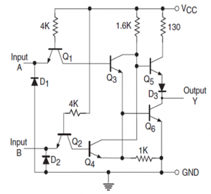
Suppose input A is at logic high, corresponding transistor’s emitter-base junction is reverse biased, and base-collector junction is forward biased. Transistor Q3 gets base current from supply voltage Vcc and goes to saturation. As a result of low collector voltage from Q3, transistor Q5 goes to cut off and on the other hand, if another input is low, Q4 is cut off and correspondingly Q5 is cut off and output is connected directly to ground through transistor Q3. Similarly, when both inputs are logic low, the output will be at logic high.
2. NOT
Gate![TTL 4]()
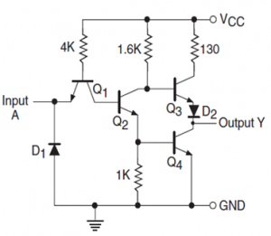
When the input is low, the corresponding base-emitter junction is forward biased, and the base-collector junction is reverse biased. As a result transistor Q2 is cut off and also transistor Q4 is cut off. Transistor Q3 goes to saturation and diode D2 starts conducting and output is connected to Vcc and goes to logic high. Similarly, when input is at logic high, the output is at logic low.
Share This Post: